Browse by tag:
DESCRIPTION
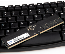
NTBSD5P48SP-16 is a 2G x8 1R x 64-Bit (16GB) fifth-generation
double data rate (DDR5) SDRAM (Synchronous DRAM) memory
module, based on eight 2G x 8-bit FBGA components per module.
The SPD is programmed to JEDEC standard latency DDR5-4800
timing of 40-40-40 at 1.1V. Each 288-pin DIMM uses gold contact
fingers. The electrical and mechanical specifications are as follows:
FEATURES
• VDD/VDDQ = 1.1V Typical
• VPP = 1.8V Typical
• 32 Bank with x4/x8
• 16 Bank with x16
• 8 BG(Bank Group) for X4/X8/X16 configurations
• BL16, BC8 OTF, BL32, BL32 OTF supported
• Temperature Encoding
• Same Bank Refresh
• Hard/Soft Post Package Repair
• Input Clock Frequency Change
• Maximum Power Saving Mode (MPSM)
• Multi-Purpose Command (MPC)
• Per DRAM Addressability (PDA)
• Connectivity Test (CT) / ZQ Calibration
• DFE (Decision Feedback Equalization) for DQ
• DQS Interval Oscillator
• 1N / 2N Mode support for Commands
• On-Die ECC
• ECC Transparency and Error Scrub
• CRC (Cyclic Redundancy Check)
• Loopback for multiple purposes - monitor data, BER(Bit Error
Rate) analysis, etc.
• Package Output Driver Test Mode
• Training Modes:
• VrefDQ / VrefCA / VrefCS Training
• Read Training Mode
• CA Training Mode
• CS Training Mode
• Per Pin VREFDQ Training
• Write Leveling Training Mode
• Duty Cycle Adjuster (DCA) for Read – Global
• Per Pin DCA(Duty Cycle Adjuster) for Read - Per
Pin(DQ)
• PCB: Height 1.23” (31.25mm)
• RoHS Compliant and Halogen-Free
SPECIFICATIONS
CL(CAS Latency) 40 cycles
tRCD(RAS to CAS Delay) 40 cycles
tRP(RAS Precharge Time) 40 cycles
tRAS(RAS Active Time) 77 cycles
Maximum Operating Power TBD W*
Operating Temperature 0o C to +70o C
Storage Temperature -40o C to +85o C
*Power will vary depending on the SDRAM used.


